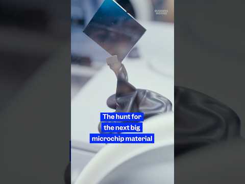
How #researchers at #Intel are inventing the next generation of #chips. #tech #madeinamerica

Video thumbnail: How #researchers at #Intel are inventing the next generation of #chips. #tech #madeinamerica
Jul 2, 20261m 53s video lengthBusiness Insider

The Signal

Researchers are currently aggressively testing alternative materials to surpass silicon, which has enabled decades of semiconductor progress but is now hitting fundamental scaling limits. Because the development cycle for next-generation channel devices spans five to ten years, teams must manage an experimental pipeline that expects massive attrition long before a product ever arrives.

The Case

Experimental Pipeline

  • The research process is intentionally designed to handle high failure rates, with labs running what the speaker calls millions of experiments to test candidate materials.0:48
  • Only an estimated 10% to 25% of these experimental candidates successfully transition into actual, market-ready products.1:35
  • Development is structured to begin 5–10 years before the devices reach the market to account for the slow, methodical transition required to move materials from bench-scale testing to fab-scale manufacturing.

Management Strategy

  • Facing deep uncertainty about which specific material will eventually win, the lab's primary decision function is to maintain a broad portfolio of options rather than betting early on a single path.
  • Down-selection serves as a critical filtration mechanism, where researchers identify the most promising elements from their experimental 'playground' before committing them to high-cost fab validation.1:05

The 1 Minute Signal Take

This work highlights the inherent friction between high-risk basic research and the rigid timeline of commercial hardware development. The high failure rate underscores that the primary output of this stage is not a finished product, but the preservation of multiple technological paths to insulate the industry against future scaling blocks.

Pro Analysis

Why It Matters

As silicon approaches physical scaling limits, the entire global economy faces a bottleneck. This research provides a rare, honest look at the 'attrition-based' methodology employed by legacy giants to navigate a future where Moore's Law no longer reliably provides performance gains.

Strategic Implications

Companies relying on chip advancement must prepare for higher volatility in material availability and longer R&D cycles. The shift to a diversified material strategy suggests that future chip performance will stem from specialized material stacks rather than uniform silicon structures.

Evidence & Hype Audit

This is moderate-trust content. It correctly frames R&D realities regarding attrition and long timelines, but lacks hard physical constraints or specific material data. It is a high-level framing of institutional strategy rather than a technical deep dive.

Counterarguments

Critics might argue that such large, siloed corporate labs struggle to out-innovate agile materials startups. Additionally, the insistence on internal portfolio management may mask an inability to pivot quickly if a new material breakthrough happens outside of their internal 'funnel.'

Role-Specific Takeaways

  • Investors: Monitor R&D spend as a proxy for long-term options preservation rather than near-term output.
  • System Architects: Expect higher-variance hardware characteristics in the coming decade.
  • Material Scientists: Focus on materials capable of scaling through the transition from lab-based proof-of-concept to fab-scale mass production.

What to Do Next

  • Map your long-term product roadmaps to a 10-year horizon for component availability.
  • Investigate which material-science alliances or partnerships could mitigate the high failure risk of solo R&D.
  • Diversify technology foundations to avoid dependency on a single semiconductor material class.
  • Prioritize modularity in architecture to allow for late-stage material swaps.

Share this

Tags