
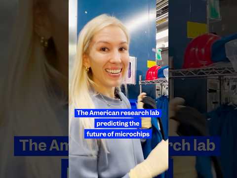
Why It Matters
The transition to new material sets represents a pivot point for the entire semiconductor industry. If current materials are indeed reaching their atomic limits, the industry is entering a post-scaling era where performance gains will rely on chemical engineering rather than lithographic shrinking.
Strategic Implications
Intel is investing in a high-risk, long-horizon play. By focusing on materials discovery 5-10 years out, they are attempting to define the 'next big' process standard, which could allow them to lock in a manufacturing advantage once Moore’s Law-style shrinking hits a terminal wall.
Evidence & Hype Audit
This content is high-level and promotional. It effectively captures the 'what' and 'why' (atomic limits, research focus) but lacks the 'how' or specific validation. The reference to the 'periodic table' is clearly narrative, not scientific proof of progress. Trust this as a signal of intent, not an evidence-based roadmap.
Counterarguments
Critics might argue that such long-term research is too detached from commercial reality, especially when the company faces immediate competitive pressure. Furthermore, relying on 'new materials' (often exotic elements) can introduce immense supply chain volatility compared to the established global silicon ecosystem.
Role-Specific Takeaways
- Investors: View this as a bellwether for long-term R&D health, but do not price in immediate commercial impact.
- Engineers: Observe the move toward extreme contamination-controlled environments as a baseline for future material labs.
- Policy Makers: Understand that future-proofing the domestic supply chain requires deep materials science, not just fab capacity.
What To Do Next
- Investigate which material categories (e.g., beyond-silicon semiconductors) are currently moving from lab to pilot line.
- Analyze patent filings related to 'atomic layer deposition' or similar processes to ground the 'new materials' claims.
- Monitor industry forums for reports on the thermal stability of experimental chip materials.
- Track hiring patterns at top-tier research labs for insights into which specific disciplines are being prioritized.